







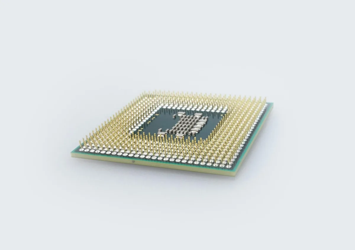
A team of international researchers has successfully demonstrated a new method for stacking three layers of single-crystalline silicon to create high-performance 3D circuits, marking a significant breakthrough in semiconductor manufacturing. Published recently in leading scientific journals, this development offers a viable path to bypass the physical limitations of traditional 2D chip architecture, potentially extending Moore’s Law for years to come.
The End of Traditional Scaling
For decades, the semiconductor industry has relied on Moore’s Law, the observation that the number of transistors on a microchip doubles approximately every two years. As transistors have shrunk to the nanometer scale, however, manufacturers have hit a